<--- Back to Details
First PageDocument Content
Thin film deposition / Industrial gases / Semiconductor growth / Semiconductor device fabrication / Molecular beam epitaxy / Gallium arsenide / Liquid nitrogen / High-electron-mobility transistor / Water cooling / Epitaxy / Nitrogen / Metalorganic vapour phase epitaxy
Date: 2009-05-08 06:40:08
Thin film deposition
Industrial gases
Semiconductor growth
Semiconductor device fabrication
Molecular beam epitaxy
Gallium arsenide
Liquid nitrogen
High-electron-mobility transistor
Water cooling
Epitaxy
Nitrogen
Metalorganic vapour phase epitaxy

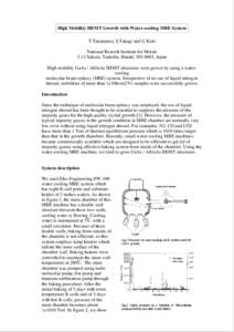
High Mobility HEMT Growth with Water-cooling MBE System T.Takamatsu, S.Takagi and G.Kido National Reserch Institute for Metals 3-13 Sakura, Tsukuba, Ibaraki, Japan High mobility GaAs / AlGaAs HEMT structures wer
Add to Reading List

Source URL: www.1974eiko.co.jp

Download Document from Source Website

File Size: 31,85 KB

Share Document on Facebook

Similar Documents

Nickel enhanced graphene growth directly on dielectric substrates by molecular beam epitaxy
					Nickel enhanced graphene growth directly on dielectric substrates by molecular beam epitaxy

Nickel enhanced graphene growth directly on dielectric substrates by molecular beam epitaxy Nickel enhanced graphene growth directly on dielectric substrates by molecular beam epitaxy

DocID: 1sbdn - View Document

Structure and tunnel magnetoresistance in Fe/MgF2/Co junctions With an oxide seed layer on an Fe bottom electrode S. Mitani,a) T.Moriyama, and K.Takanashi Institute for Mterials Research, Tohoku University, Sendai

Structure and tunnel magnetoresistance in Fe/MgF2/Co junctions With an oxide seed layer on an Fe bottom electrode S. Mitani,a) T.Moriyama, and K.Takanashi Institute for Mterials Research, Tohoku University, Sendai

DocID: 1r2YY - View Document

High Mobility HEMT Growth with Water-cooling MBE System T.Takamatsu, S.Takagi and G.Kido National Reserch Institute for Metals 3-13 Sakura, Tsukuba, Ibaraki, Japan High mobility GaAs / AlGaAs HEMT structures wer
High Mobility HEMT Growth with Water-cooling MBE System T.Takamatsu, S.Takagi and G.Kido National Reserch Institute for Metals 3-13 Sakura, Tsukuba, Ibaraki, Japan High mobility GaAs / AlGaAs HEMT structures wer

DocID: 1puFe - View Document

Comparison of the growth kinetics of In2O3 and Ga2O3 and their suboxide desorption during plasma-assisted molecular beam epitaxy Patrick Vogt and Oliver Bierwagen Citation: Applied Physics Letters 109, ); doi

Comparison of the growth kinetics of In2O3 and Ga2O3 and their suboxide desorption during plasma-assisted molecular beam epitaxy Patrick Vogt and Oliver Bierwagen Citation: Applied Physics Letters 109, ); doi

DocID: 1oJBU - View Document

Materials Physics and Mechanics288  Received: November 6, 2015 MOLECULAR BEAM EPITAXY GROWN STRAINED HETEROSTRUCTURES FOR ACTIVE REGION OF LASER DIODE

Materials Physics and Mechanics288 Received: November 6, 2015 MOLECULAR BEAM EPITAXY GROWN STRAINED HETEROSTRUCTURES FOR ACTIVE REGION OF LASER DIODE

DocID: 1nNHq - View Document