| Document Date: 2010-01-26 01:21:50
Open Document File Size: 927,03 KBShare Result on Facebook
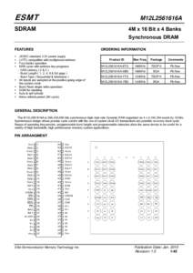
Company BLOCK DIAGRAM CKE Clock Generator Bank / A6 / CA8 BA1 / Refresh Counter Row Decoder CLK Bank / Elite Semiconductor Memory Technology Inc. / BT / A6 A5 A4 VSS Elite Semiconductor Memory Technology Inc. / BA0 Bank Select / / Facility stable Unit Note mA / / IndustryTerm bank active command / bank address / bank read/write command / idle bank / bank activation / bank / memory system applications / / Organization Parameter Value Unit / International Criminal Court / / Person Max Freq / / Position Colonel / Pb-free M12L2561616A-7BG 143MHz BGA Pb-free GENERAL / / ProgrammingLanguage DC / L / / Technology RAM / SDRAM / Output Buffer RAS Column Latch Circuit CS Control Logic Command Decoder Sense Amplifier DQ PIN DESCRIPTION PIN NAME CLK System Clock CS Chip / /
SocialTag |

